5.1 Principles of I/O Hardware
Different people look at I/O hardware in different ways. Electrical engineers look at it in terms of chips, wires, power supplies, motors, and all the other physical components that comprise the hardware. Programmers look at the interface presented to the software—the commands the hardware accepts, the functions it carries out, and the errors that can be reported back. In this book, we are concerned with programming I/O devices, not designing, building, or maintaining them, so our interest is in how the hardware is programmed, not how it works inside. Nevertheless, the programming of many I/O devices is often intimately connected with their internal operation. In the next three sections, we will provide a little general background on I/O hardware as it relates to programming. It may be regarded as a review and expansion of the introductory material in Sec. 1.3.
5.1.1 I/O Devices
I/O devices can be roughly divided into two categories: block devices and character devices. A block device is one that stores information in fixed-size blocks, each one with its own address. Common block sizes range from 512 to 65,536 bytes. All transfers are in units of one or more entire (consecutive) blocks. The essential property of a block device is that it is possible to read or write each block independently of all the other ones. Hard disks and SSDs (Solid State Drives) are common block devices, and so are magnetic tape drives that are now commonly found in computer museums but are also still in use in data centers and have been the go-to solution for really big mass storage for over half a century. An LTO-8 Ultrium tape, for example, can store 12 TB, be read at 750 MB/s, and is expected to last 30 years. It costs under $100.
The other type of I/O device is the character device. A character device delivers or accepts a stream of characters, without regard to any block structure. It is not addressable and does not have a seek operation. Printers, network interfaces, mice (for pointing), rats (for psychology lab experiments), and most other devices that are not disk-like can be seen as character devices.
This classification scheme is not perfect. Some devices do not fit in. Clocks, for example, are not block addressable. Nor do they generate or accept character streams. All they do is cause interrupts at well-defined intervals. Memory-mapped screens do not fit the model well either. Nor do touch screens, for that matter. Still, the model of block and character devices is general enough that it can be used as a basis for making some of the operating system software dealing with I/O device independent. The file system, for example, deals just with abstract block devices and leaves the device-dependent part to lower-level software.
I/O devices cover a huge range in speeds, which puts considerable pressure on the software to perform well over many orders of magnitude in data rates. Figure 5-1 shows the data rates of some common devices.
Figure 5-1
| Device | Data rate |
|---|---|
| Keyboard | 10 bytes/sec |
| Mouse | 100 bytes/sec |
| 56K modem | 7 KB/sec |
| Bluetooth 5 BLE | 256 KB/sec |
| Scanner at 300 dpi | 1 MB/sec |
| Digital video recorder | 3.5 MB/sec |
| 802.11n Wireless | 37.5 MB/sec |
| USB 2.0 | 60 MB/sec |
| 16x Blu-ray disc | 72 MB/sec |
| Gigabit Ethernet | 125 MB/sec |
| SATA 3 disk drive | 600 MB/sec |
| USB 3.0 | 625 MB/sec |
| Single-lane PCIe 3.0 bus | 985 MB/sec |
| 802.11ax Wireless | 1.25 GB/sec |
| PCIe Gen 3.0 NVMe M.2 SSD (reading) | 3.5 GB/sec |
| USB 4.0 | 5 GB/sec |
| PCI Express 6.0 | 126 GB/sec |
Some typical device, network, and bus data rates.
5.1.2 Device Controllers
I/O units often consist of a mechanical component and an electronic component. It is possible to separate the two parts to provide a more modular and general design. The electronic component is called the device controller or adapter. On personal computers, it often takes the form of a chip on the motherboard or a printed circuit card that can be inserted into a (PCIe) expansion slot. The mechanical component is the device itself. This arrangement is shown in Fig. 1-6.
The controller card usually has a connector on it, into which a cable leading to the device itself can be plugged. Many controllers can handle two, four, eight, or even more identical devices. If the interface between the controller and device is a standard interface, either an official ANSI, IEEE, or ISO standard or a de facto one, then companies can make controllers or devices that fit that interface. Many companies, for example, make disk drives that match the SATA, SCSI, USB, or Thunderbolt, interfaces.
The interface between the controller and the device is often a very low-level one. A disk, for example, might have 3,000,000 tracks, each formatted with between 200 and 500 sectors of 4,096 bytes each. What actually comes off the drive, however, is a serial bit stream, starting with a preamble, then followed by the in a sector, and finally a checksum, or ECC (Error-Correcting Code). The preamble is written when the disk is formatted and contains the cylinder and sector number, the sector size, and similar data, as well as synchronization information.
The controller’s job is to convert the serial bit stream into a block of bytes and perform any error correction that is necessary. The block of bytes is typically first assembled, bit by bit, in a buffer inside the controller. After its checksum has been verified and the block has been declared to be error free, it can then be copied to main memory.
The controller for an LCD display monitor also works as a bit serial device at an equally low level. It reads bytes containing the characters to be displayed from memory and generates the signals to modify the polarization of the backlight for the corresponding pixels in order to write them on screen. If it were not for the display controller, the operating system programmer would have to explicitly program the electric fields of all pixels. With the controller, the operating system initializes the controller with a few parameters, such as the number of characters or pixels per line and number of lines per screen, and lets the controller take care of actually driving the electric fields.
In a very short time, LCD screens have completely replaced the old CRT (Cathode Ray Tube) monitors. CRT monitors fire a beam of electrons onto a fluorescent screen. Using magnetic fields, the system is able to bend the beam and draw pixels on the screen. Compared to LCD screens, CRT monitors were bulky, power hungry, and fragile. Moreover, the resolution on today’s (Retina) LCD screens is so good that the human eye is unable to distinguish individual pixels. It is hard to imagine today that laptops in the past came with a small CRT screen that made them more than 20 cm deep with a nice work-out weight of around 12 kg.
5.1.3 Memory-Mapped I/O
Each controller has a few registers that are used for communicating with the CPU. By writing into these registers, the operating system can command the device to deliver data, accept data, switch itself on or off, or otherwise perform some action. By reading from these registers, the operating system can learn what the device’s state is, whether it is prepared to accept a new command, and so on.
In addition to the control registers, many devices have a data buffer that the operating system can read and write. For example, a common way for computers to display pixels on the screen is to have a video RAM, which is basically just a data buffer, available for programs or the operating system to write into.
The issue thus arises of how the CPU communicates with the control registers and also with the device data buffers. Two alternatives exist. In the first approach, each control register is assigned an I/O port number, an 8- or 16-bit integer. The set of all the I/O ports form the I/O port space, which is protected so that ordinary user programs cannot access it (only the operating system can). Using a special I/O instruction such as
IN REG,PORT,
the CPU can read in control register PORT and store the result in CPU register REG. Similarly, using
OUT PORT,REG
the CPU can write the contents of REG to a control register. Most early computers, including nearly all mainframes, such as the IBM 360 and all of its successors, worked this way.
In this scheme, the address spaces for memory and I/O are different, as shown in Fig. 5-2(a). The instructions
Figure 5-2
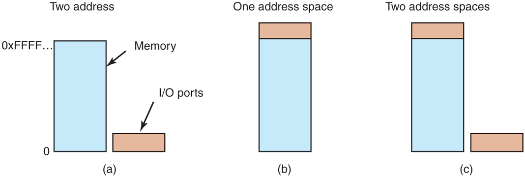
(a) Separate I/O and memory space. (b) Memory-mapped I/O. (c) Hybrid.
IN R0,4and
MOV R0,4are completely different in this design. The former reads the contents of I/O port 4 and puts it in R0, whereas the latter reads the contents of memory word 4 and puts it in R0. The 4s in these examples refer to different and unrelated address spaces.
The second approach, introduced with the PDP-11, is to map all the control registers into the memory space, as shown in Fig. 5-2(b). Each control register is assigned a unique memory address to which no memory is assigned. This system is called memory-mapped I/O. In most systems, the assigned addresses are at or near the top of the address space. A hybrid scheme, with memory-mapped I/O data buffers and separate I/O ports for the control registers, is shown in Fig. 5-2(c). The x86 uses this architecture, with addresses 640K to 1M – 1 being reserved for device data buffers in IBM PC compatibles, in addition to I/O ports 0 to 64K – 1.
As an aside, assigning 360K addresses for I/O devices on the original PC was an absurdly large number and limited the amount of memory that could be put on a PC. Having 4K I/O addresses would have been plenty. But back when memory cost $1 per byte, no one thought that anyone would want to have 640 KB on a PC, let alone 900 KB or more. What the designers did not realize was how fast memory prices would tumble. Nowadays, you would be hard pressed to find a notebook computer with less than 4,000,000 KB of RAM.
How do these schemes actually work in practice? In all cases, when the CPU wants to read a word, either from memory or from an I/O port, it puts the address it needs on the bus’ address lines and then asserts a READ signal on a bus’ control line. A second signal line is used to tell whether I/O space or memory space is needed. If it is memory space, the memory responds to the request. If it is I/O space, the I/O device responds to the request. If there is only memory space [as in Fig. 5-2(b)], every memory module and every I/O device compares the address lines to the range of addresses that it services. If the address falls in its range, it responds to the request. Since no address is ever assigned to both memory and an I/O device, there is no ambiguity and no conflict.
These two schemes for addressing the controllers have different strengths and weaknesses. Let us start with the advantages of memory-mapped I/O. First of all, if special I/O instructions are needed to read and write the device control registers, access to them requires the use of assembly code since there is no way to execute an IN or OUT instruction in C or C++. Calling such a procedure adds overhead to controlling I/O. In contrast, with memory-mapped I/O, device control registers are just variables in memory and can be addressed in C the same way as any other variables. Thus, with memory-mapped I/O, an I/O device driver can be written entirely in C. Without memory-mapped I/O, some assembly code is needed.
Second, with memory-mapped I/O, no special protection mechanism is needed to keep user processes from performing I/O. All the operating system has to do is refrain from putting that portion of the address space containing the control registers in any user’s virtual address space. Even better yet, if each device has its control registers on a different page of the address space, the operating system can give a user control over specific devices but not others by simply including the desired pages in its page table. Such a scheme can allow different device drivers to be run in different user-mode address spaces, not only reducing kernel size but also keeping one driver from interfering with others. This also prevents a driver crash from taking down the entire system. Some microkernels (e.g., MINIX 3) work like this.
Third, with memory-mapped I/O, every instruction that can reference memory can also reference control registers. For example, if there is an instruction, TEST, that tests a memory word for 0, it can also be used to test a control register for 0, which might be the signal that the device is idle and can accept a new command. The assembly language code might look like this:
LOOP: TEST PORT_4 // check if port 4 is 0BEQ READY // if it is 0, go to readyBRANCH LOOP // otherwise, continue testingREADY:
If memory-mapped I/O is not present, the control register must first be read into the CPU, then tested, requiring two instructions instead of just one. In the case of the loop given above, a fourth instruction has to be added, slightly slowing down the responsiveness of detecting an idle device.
In computer design, practically everything involves trade-offs, and that is the case here, too. Memory-mapped I/O also has its disadvantages. First, most computers nowadays have some form of caching of memory words. Caching a device control register would be disastrous. Consider the assembly-code loop given above in the presence of caching. The first reference to PORT_4 would cause it to be cached. Subsequent references would just take the value from the cache and not even ask the device. Then when the device finally became ready, the software would have no way of finding out. Instead, the loop would go on forever.
To prevent this situation with memory-mapped I/O, the hardware has to be able to selectively disable caching, for example, on a per-page basis. This feature adds extra complexity to both the hardware and the operating system, which has to manage the selective caching.
Second, if there is only one address space, then all memory modules and all I/O devices must examine all memory references to see which ones to respond to. If the computer has a single bus, as in Fig. 5-3(a), having everyone look at every address is straightforward.
Figure 5-3
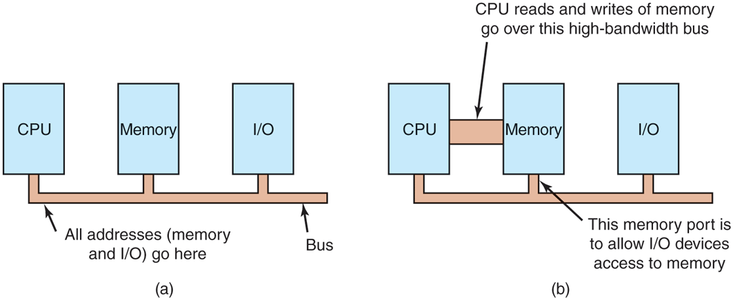
(a) A single-bus architecture. (b) A dual-bus memory architecture.
However, the trend in modern personal computers is to have a dedicated highspeed memory bus, as shown in Fig. 5-3(b). The bus is tailored to optimize memory performance, with no compromises for the sake of slow I/O devices. x86 systems can have multiple buses (memory, PCIe, SCSI, and USB), as shown in Fig. 1-12.
The trouble with having a separate memory bus on memory-mapped machines is that the I/O devices have no way of seeing memory addresses as they go by on the memory bus, so they have no way of responding to them. Again, special measures have to be taken to make memory-mapped I/O work on a system with multiple buses. One possibility is to first send all memory references to the memory. If the memory fails to respond, then the CPU tries the other buses. This design can be made to work but requires additional hardware complexity.
A second possible design is to put a snooping device on the memory bus to pass all addresses presented to potentially interested I/O devices. The problem here is that I/O devices may not be able to process requests at the speed the memory can.
A third possible design, and one that would well match the design sketched in Fig. 1-12, is to filter addresses in the memory controller. In that case, the memory controller chip contains range registers that are preloaded at boot time. For example, 640K to 1M ‒ 1 could be marked as a nonmemory range. Addresses that fall within one of the ranges marked as nonmemory are forwarded to devices instead of to memory. The main disadvantage of this scheme is the need for figuring out at boot time which memory addresses are not really memory addresses. Thus each scheme has arguments for and against it, so compromises and trade-offs are inevitable, especially when backward compatibility with legacy systems is important.
5.1.4 Direct Memory Access
No matter whether a CPU does or does not have memory-mapped I/O, it needs to address the device controllers to exchange data with them. The CPU can request data from an I/O controller one byte at a time, but doing so wastes the CPU’s time, so a different scheme, called DMA (Direct Memory Access) is often used. To simplify the explanation, we assume that the CPU accesses all devices and memory via a single system bus that connects the CPU, the memory, and the I/O devices, as shown in Fig. 5-4. We already know that the real organization in modern systems is more complicated, but all the principles are the same. The operating system can only use DMA if the hardware has a DMA controller, which most systems do. Sometimes this controller is integrated into disk controllers and other controllers, but such a design requires a separate DMA controller for each device. More commonly, a single DMA controller is available (e.g., on the motherboard) for regulating transfers to multiple devices, often concurrently.
Figure 5-4
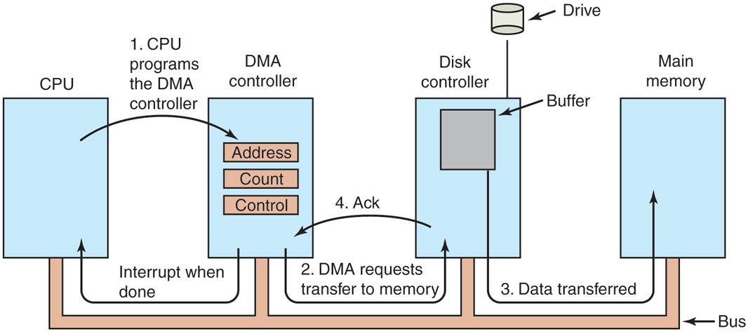
Operation of a DMA transfer.
No matter where it is physically located, the DMA controller has access to the system bus independent of the CPU, as shown in Fig. 5-4. It contains several registers that can be written and read by the CPU. These include a memory address register, a byte count register, and one or more control registers. The control registers specify the I/O port to use, the direction of the transfer (reading from the I/O device or writing to the I/O device), the transfer unit (byte at a time or word at a time), and the number of bytes to transfer in one burst.
To explain how DMA works, consider how data are read from, say, a disk. Let us first look at how disk reads occur when DMA is not used. First, the disk controller reads the block (one or more sectors) from the drive serially, bit by bit, until the entire block is stored in the controller’s internal buffer. Next, it computes the checksum to verify that no read errors have occurred. Then the controller causes an interrupt. When the operating system starts running, it can read the disk block from the controller’s buffer a byte or a word at a time by executing a loop, with each iteration reading one byte or word from a controller device register and storing it in main memory.
When DMA is used, the procedure is different. First the CPU programs the DMA controller by setting its registers so it knows what to transfer where (step 1 in Fig. 5-4). It also issues a command to the disk controller telling it to read data from the disk into its internal buffer and verify the checksum. When valid data are in the disk controller’s buffer, DMA can begin.
The DMA controller initiates the transfer by issuing a read request over the bus to the disk controller (step 2). This read request looks like any other read request, and the disk controller does not know (or care) whether it came from the CPU or from a DMA controller. Typically, the memory address to write to is on the bus’ address lines, so when the disk controller fetches the next word from its internal buffer, it knows where to write it. The write to memory is another standard bus cycle (step 3). When the write is complete, the disk controller sends an acknowledgement signal to the DMA controller, also over the bus (step 4). The DMA controller then increments the memory address to use and decrements the byte count. If the byte count is still greater than 0, steps 2 through 4 are then repeated until the count reaches 0. At that time, the DMA controller interrupts the CPU to let it know that the transfer is now complete. When the operating system starts up, it does not have to copy the disk block to memory; it is already there.
DMA controllers vary considerably in their sophistication. The simplest ones handle one transfer at a time, as described above. More complex ones can be programmed to handle multiple transfers at the same time. Such controllers have multiple sets of registers internally, one for each channel. The CPU starts by loading each set of registers with the relevant parameters for its transfer. Each transfer must use a different device controller. After each word is transferred (steps 2 through 4) in Fig. 5-4, the DMA controller decides which device to service next. It may be set up to use a round-robin algorithm, or it may have a priority scheme design to favor some devices over others. Multiple requests to different device controllers may be pending at the same time, provided that there is an unambiguous way to tell the acknowledgements apart. Often a different acknowledgement line on the bus is used for each DMA channel for this reason.
Many buses can operate in two modes: word-at-a-time mode and block mode. Often, DMA controllers can also operate in either mode. In the former mode, the operation is as described above: the DMA controller requests the transfer of one word and gets it. If the CPU also wants the bus, it has to wait. The mechanism is called cycle stealing because the device controller sneaks in and steals an occasional bus cycle from the CPU once in a while, delaying it slightly. In block mode, the DMA controller tells the device to acquire the bus, issue a series of transfers, then release the bus. This form of operation is called burst mode. It is more efficient than cycle stealing because acquiring the bus takes time and multiple words can be transferred for the price of one bus acquisition. The downside to burst mode is that it can block the CPU and other devices for a substantial period if a long burst is being transferred.
In the model we have been discussing, sometimes called fly-by mode, the DMA controller tells the device controller to transfer the data directly to main memory. An alternative mode that some DMA controllers use is to have the device controller send the word to the DMA controller, which then issues a second bus request to write the word to wherever it is supposed to go. This scheme requires an extra bus cycle per word transferred, but is more flexible in that it can also perform device-to-device copies and even memory-to-memory copies (by first issuing a read to memory and then issuing a write to memory at a different address).
Most DMA controllers use physical memory addresses for their transfers. Using physical addresses requires the operating system to convert the virtual address of the intended memory buffer into a physical address and write this physical address into the DMA controller’s address register. An alternative scheme used in a few DMA controllers is to write virtual addresses into the DMA controller instead. Then the DMA controller must use the MMU to have the virtual-to-physical translation done. Only when the MMU is part of the memory (possible, but rare), rather than part of the CPU, can virtual addresses be put on the bus. In Chap. 7, we will see that an IOMMU (an MMU for I/O) offers similar functionality: it translates the virtual addresses used by devices to physical addresses. In other words, the virtual address of a buffer used by a device may be different from the virtual address used for the same buffer by the CPU, while both are different from the corresponding physical address.
We mentioned earlier that before DMA can start, the disk first reads data into its internal buffer. You may be wondering why the controller does not just store the bytes in main memory as soon as it gets them from the disk. In other words, why does it need an internal buffer? There are two reasons. First, by doing internal buffering, the disk controller can verify the checksum before starting a transfer. If the checksum is incorrect, an error is signaled and no transfer is done.
The second reason is that once a disk transfer has started, the bits keep arriving from the disk at a constant rate, whether the controller is ready for them or not. If the controller tried to write data directly to memory, it would have to go over the system bus for each word transferred. If the bus were busy due to some other device using it (e.g., in burst mode), the controller would have to wait. If the next disk word arrived before the previous one had been stored, the controller would have to store it somewhere. If the bus were very busy, the controller might end up storing quite a few words and having a lot of administration to do as well. When the block is buffered internally, the bus is not needed until the DMA begins, so the design of the controller is much simpler because the DMA transfer to memory is not time critical. (Some older controllers did, in fact, go directly to memory with only a small amount of internal buffering, but when the bus was very busy, a transfer might have had to be terminated with a buffer overrun error.)
Some computers do not use DMA. The argument against it might be that the main CPU is often far faster than the DMA controller and can do the job much faster (when the limiting factor is not the speed of the I/O device). If there is no other work for it to do, having the (fast) CPU wait for the (slow) DMA controller to finish is pointless. Also, getting rid of the DMA controller and having the CPU do all the work in software saves money, important on low-end (embedded) computers.
5.1.5 Interrupts Revisited
We briefly introduced interrupts in Sec. 1.3.4, but there is more to be said. Before we start, you should know that the literature is confusing when it comes to interrupts. Textbooks and Web pages may use the term to refer to hardware interrupts, traps, exceptions, faults, and a few other things. What do these terms mean? We generally use trap to refer to a deliberate action by the program code, for instance, a trap into the kernel for a system call. A fault or exception is similar, except that it is generally not deliberate. For instance, the program may trigger a segmentation fault when it tries to access memory that it is not allowed to access or wants to learn what 100 divided by zero is. In contrast, we will now talk mostly about hardware interrupts, where a device such as printer or a network sends a signal to the CPU. The reason all these terms are frequently clubbed together is that they are handled in similar ways, even if they are triggered differently. In this section, we look at the hardware side. In Section 5.3, we will turn to the further handling of interrupts by the software.
Figure 5-5 shows the interrupt structure in a typical personal computer system. In this respect, a smartphone or tablet works the same way. At the hardware level, interrupts work as follows. When an I/O device has finished the work given to it, it causes an interrupt (assuming that interrupts have been enabled by the operating system), by asserting a signal on a bus line that it has been assigned. This signal is detected by the interrupt controller chip on the motherboard, which then decides what to do.
Figure 5-5
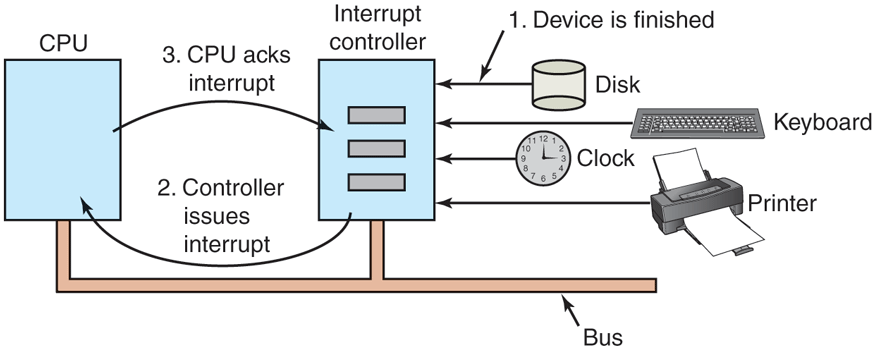
How an interrupt happens. The connections between the devices and the controller actually use interrupt lines on the bus rather than dedicated wires.
If no other interrupts are pending, the interrupt controller handles the interrupt immediately. However, if another interrupt is in progress, or another device has made a simultaneous request on a higher-priority interrupt request line on the bus, the device is just ignored for the moment. In this case, it continues to assert an interrupt signal on the bus until it is serviced by the CPU.
To handle the interrupt, the controller puts a number on the address lines specifying which device wants attention and asserts a signal to interrupt the CPU.
The interrupt signal causes the CPU to stop what it is doing and start doing something else. The number on the address lines is used as an index into a table called the interrupt vector to fetch a new program counter. This program counter points to the start of the corresponding interrupt-service procedure. Typically traps, exceptions, and interrupts use the same mechanism from this point on, often sharing the same interrupt vector. The location of the interrupt vector can be hardwired into the machine or it can be anywhere in memory, with a CPU register (loaded by the operating system) pointing to its origin.
Shortly after it starts running, the interrupt-service procedure acknowledges the interrupt by writing a certain value to one of the interrupt controller’s I/O ports. This acknowledgement tells the controller that it is free to issue another interrupt. By having the CPU delay this acknowledgement until it is ready to handle the next interrupt, race conditions involving multiple (almost simultaneous) interrupts can be avoided. As an aside, some (older) computers do not have a centralized interrupt controller, so each device controller requests its own interrupts.
The hardware always saves certain information before starting the service procedure. Which information is saved and where it is saved vary greatly from CPU to CPU. As a bare minimum, the program counter must be saved, so the interrupted process can be restarted. At the other extreme, all the visible registers and a large number of internal registers may be saved as well.
Another issue is where to save this information. One option is to put it in internal registers that the operating system can read out as needed. However, a problem with this approach is that the interrupt controller cannot be acknowledged until all potentially relevant information has been read out, lest a second interrupt overwrite the internal registers saving the state. This strategy leads to long dead times when interrupts are disabled and possibly to lost interrupts and lost data.
Consequently, most CPUs save the information on the stack. However, this approach, too, has problems. To start with: whose stack? If the current stack is used, it may well be a user process stack. The stack pointer may not even be legal, which would cause a fatal error when the hardware tried to write some words at the address pointed to. Also, it might point near the end of a page. After several memory writes, the page boundary might be exceeded and a page fault generated. Having a page fault occur during the hardware interrupt processing creates a bigger problem: where to save the state to handle the page fault?
If the kernel stack is used, there is a much better chance of the stack pointer being legal and pointing to a pinned page. However, switching into kernel mode may require changing MMU contexts and will probably invalidate most or all of the cache and TLB. Reloading all of these, statically or dynamically, will increase the time to process an interrupt and thus waste CPU time at a critical moment.
So far, we have discussed interrupt handling mostly from a hardware perspective. However, there is a lot of software involved in I/O also. We will look at the I/O software stack in detail in Sec. 5.3.
Precise and Imprecise Interrupts
Another problem is caused by the fact that most modern CPUs are heavily pipelined and often superscalar (internally parallel). In older systems, after each instruction was finished executing, the microprogram or hardware checked to see if there was an interrupt pending. If so, the program counter and PSW were pushed onto the stack and the interrupt sequence begun. After the interrupt handler ran, the reverse process took place, with the old PSW and program counter popped from the stack and the previous process continued.
This model makes the implicit assumption that if an interrupt occurs just after some instruction, all the instructions up to and including that instruction have been executed completely, and no instructions after it have executed at all. On older machines, this assumption was always valid. On modern ones it may not be.
For starters, consider the pipeline model of Fig. 1-7(a). What happens if an interrupt occurs while the pipeline is full (the usual case)? Many instructions are in various stages of execution. When the interrupt occurs, the value of the program counter may not reflect the correct boundary between executed instructions and nonexecuted instructions. In fact, many instructions may have been partially executed, with different instructions being more or less complete. In this situation, the program counter most likely reflects the address of the next instruction to be fetched and pushed into the pipeline rather than the address of the instruction that just was processed by the execution unit.
On a superscalar machine, such as that of Fig. 1-7(b), things are even worse. CPU instructions may be internally decomposed into so-called micro-operations and these micro-operations may execute out of order, depending on the availability of internal resources such as functional units and registers (see also Sec. 2.5.9). At the time of an interrupt, some instructions issued long ago may not be anywhere near completion and others started more recently may be (almost) done. This is not a problem as the CPU will simply buffer the results of each instruction until all previous instructions have also completed and then commit all of them in order. However, it means that at the point when an interrupt is signaled, there may be many instructions in various states of completeness, and there is not much of relation between them and the program counter at all.
An interrupt that leaves the machine in a well-defined state is called a precise interrupt (Walker and Cragon, 1995). Such an interrupt has four properties:
The PC (Program Counter) is saved in a known place.
All instructions before the one pointed to by the PC have completed.
No instruction beyond the one pointed to by the PC has finished.
The execution state of the instruction pointed to by the PC is known.
Note that even with precise interrupts there is no prohibition on instructions beyond the one pointed to by the PC from starting. It is just that any changes they make to registers or memory must be completely undone when the interrupt happens. This is what many processor architectures, including the x86, try to do. Since the CPU erases all visible effects as if these instructions never executed, we call the instructions transient. Such transient execution occurs for many reasons (Ragab et al., 2021). We already saw that a fault or interrupt that happens during the execution of an instruction while some later instructions have already completed requires the processor to throw away the results of these later instructions. However, modern CPUs employ many more tricks to improve performance. For instance, the CPU may speculate on the outcome of a conditional branch. If the outcome of an if condition was TRUE the last 50 times, the CPU will assume that it will be true the 51st time also and speculatively start fetching and executing the instructions for the TRUE branch. Of course, if the 51st time was different and the outcome is really FALSE, these instructions must now be made transient. Transient execution has been the source of all sorts of security trouble, but that is not what we need to discuss now and we save it for Chapter 9.
Meanwhile, when an interrupt occurs, what should happen to the instruction to which the PC is currently pointing? It is permitted that this instruction has been executed. It is also permitted that it has not been executed. However, it must be clear which case applies. Often, if the interrupt is an I/O interrupt, the instruction will not yet have started. However, if the interrupt is really a trap or page fault, then the PC generally points to the instruction that caused the fault so it can be restarted later. The situation of Fig. 5-6(a) illustrates a precise interrupt. All instructions up to the program counter (316) have completed and none of those beyond it have started (or have been rolled back to undo their effects).
Figure 5-6
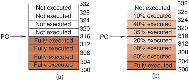
(a) A precise interrupt. (b) An imprecise interrupt.
An interrupt that does not meet these requirements is called an imprecise interrupt and makes life most unpleasant for the operating system writer, who now has to figure out what has happened and what still has to happen. Fig. 5-6(b) illustrates an imprecise interrupt, where different instructions near the program counter are in different stages of completion, with older ones not necessarily more complete than younger ones. Machines with imprecise interrupts usually vomit a large amount of internal state onto the stack to give the operating system the possibility of figuring out what was going on. The code necessary to restart the machine is typically exceedingly complicated. Also, saving a large amount of information to memory on every interrupt makes interrupts slow and recovery even worse. This leads to the ironic situation of having very fast superscalar CPUs sometimes being unsuitable for real-time work due to slow interrupts.
Some computers are designed so that some kinds of interrupts and traps are precise and others are not. For example, having I/O interrupts be precise but traps due to fatal programming errors be imprecise is not so bad since no attempt need be made to restart a running process after it has divided by zero. At that point, having done something that is infinitely bad, it is toast anyway. Some machines have a bit that can be set to force all interrupts to be precise. The downside of setting this bit is that it forces the CPU to carefully log everything it is doing and maintain shadow copies of registers so it can generate a precise interrupt at any instant. All this overhead has a major impact on performance.
Some superscalar machines, such as the x86 family, have precise interrupts to allow old software to work correctly. The price paid for backward compatibility with precise interrupts is extremely complex interrupt logic within the CPU to make sure that when the interrupt controller signals that it wants to cause an interrupt, all instructions up to some point are allowed to finish and none beyond that point are allowed to have any noticeable effect on the machine state. Here the price is paid not in time, but in chip area and in complexity of the design. If precise interrupts were not required for backward compatibility purposes, this chip area would be available for larger on-chip caches, making the CPU faster. On the other hand, imprecise interrupts make the operating system far more complicated, less secure due to the complexity, and slower, so it is hard to tell which approach is really better.
Also, as mentioned earlier, we will see in Chap. 9 that all the instructions of which the effects on the machine state have been undone (and that are therefore transient) may be problematic still from a security perspective. The reason is that not all effects are undone. In particular, they leave traces deep in the micro-architecture (where we find the cache and the TLB and other components) which an attacker may use to leak sensitive information.