1.3 Computer Hardware Review
An operating system is intimately tied to the hardware of the computer it runs on. It extends the computer’s instruction set and manages its resources. To work, it must know a great deal about the hardware, at least about how the hardware appears to the programmer. For this reason, let us briefly review computer hardware as found in modern personal computers. After that, we can start getting into the details of what operating systems do and how they work.
Conceptually, a simple personal computer can be abstracted to a model resembling that of Fig. 1-6. The CPU, memory, and I/O devices are all connected by a system bus and communicate with one another over it. Modern personal computers have a more complicated structure, involving multiple buses, which we will look at later. For the time being, this model will be sufficient. In the following sections, we will briefly review these components and examine some of the hardware issues that are of concern to operating system designers. Needless to say, this will be a very compact summary. Many books have been written on the subject of computer hardware and computer organization. Two well-known ones are by Tanenbaum and Austin (2012) and Patterson and Hennessy (2018).
Figure 1-6
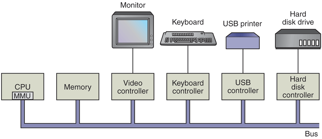
Some of the components of a simple personal computer.
1.3.1 Processors
The ‘‘brain’’ of the computer is the CPU. It fetches instructions from memory and executes them. The basic cycle of every CPU is to fetch the first instruction from memory, decode it to determine its type and operands, execute it, and then fetch, decode, and execute subsequent instructions. The cycle is repeated until the program finishes. In this way, programs are carried out.
Each CPU has a specific set of instructions that it can execute. Thus an x86 processor cannot execute ARM programs and an ARM processor cannot execute x86 programs. Please note that we will use the term x86 to refer to all the Intel processors descended from the 8088, which was used on the original IBM PC. These include the 286, 386, and Pentium series, as well as the modern Intel core i3, i5, and i7 CPUs (and their clones).
Because accessing memory to get an instruction or data word takes much longer than executing an instruction, all CPUs contain registers inside to hold key variables and temporary results. Instruction sets often contains instructions to load a word from memory into a register, and store a word from a register into memory. Other instructions combine two operands from registers and/or memory, into a result, such as adding two words and storing the result in a register or in memory.
In addition to the general registers used to hold variables and temporary results, most computers have several special registers that are visible to the programmer. One of these is the program counter, which contains the memory address of the next instruction to be fetched. After that instruction has been fetched, the program counter is updated to point to its successor.
Another register is the stack pointer, which points to the top of the current stack in memory. The stack contains one frame for each procedure that has been entered but not yet exited. A procedure’s stack frame holds those input parameters, local variables, and temporary variables that are not kept in registers.
Yet another register is the PSW (Program Status Word). This register contains the condition code bits, which are set by comparison instructions, the CPU priority, the mode (user or kernel), and various other control bits. User programs may normally read the entire PSW but typically may write only some of its fields. The PSW plays an important role in system calls and I/O.
The operating system must be fully aware of all the registers. When time multiplexing the CPU, the operating system will often stop the running program to (re)start another one. Every time it stops a running program, the operating system must save all the registers so they can be restored when the program runs later.
In fact, we distinguish between the architecture and the micro-architecture. The architecture consists of everything that is visible to the software such as the instructions and the registers. The micro-architecture comprises the implementation of the architecture. Here we find data and instruction caches, translation lookaside buffers, branch predictors, the pipelined datapath, and many other elements that should not normally be visible to the operating system or any other software.
To improve performance, CPU designers have long abandoned the simple model of fetching, decoding, and executing one instruction at a time. Many modern CPUs have facilities for executing more than one instruction at the same time. For example, a CPU might have separate fetch, decode, and execute units, so that while it is executing instruction n, it could also be decoding instruction and fetching instruction Such an organization is called a pipeline and is illustrated in Fig. 1-7(a) for a pipeline with three stages. Longer pipelines are common. In most pipeline designs, once an instruction has been fetched into the pipeline, it must be executed, even if the preceding instruction was a conditional branch that was taken. Pipelines cause compiler writers and operating system writers great headaches because they expose the complexities of the underlying machine to them and they have to deal with them.
Figure 1-7
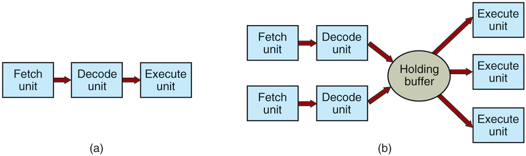
(a) A three-stage pipeline. (b) A superscalar CPU.
Even more advanced than a pipeline design is a superscalar CPU, shown in Fig. 1-7(b). In this design, multiple execution units are present, for example, one for integer arithmetic, one for floating-point arithmetic, and one for Boolean operations. Two or more instructions are fetched at once, decoded, and dumped into a holding buffer until they can be executed. As soon as an execution unit becomes available, it looks in the holding buffer to see if there is an instruction it can handle, and if so, it removes the instruction from the buffer and executes it. An implication of this design is that program instructions are often executed out of order. For the most part, it is up to the hardware to make sure the result produced is the same one a sequential implementation would have produced, but an annoying amount of the complexity is foisted onto the operating system, as we shall see.
Most CPUs, except very simple ones used in embedded systems, have (at least) two modes, kernel mode and user mode, as mentioned earlier. Usually, a bit in the PSW controls the mode. When running in kernel mode, the CPU can execute every instruction in its instruction set and use every feature of the hardware. On desktop, notebook, and server machines, the operating system normally runs in kernel mode, giving it access to the complete hardware. On most embedded systems, a small piece runs in kernel mode, with the rest of the operating system running in user mode.
User programs always run in user mode, which permits only a subset of the instructions to be executed and a subset of the features to be accessed. Generally, all instructions involving I/O and memory protection are disallowed in user mode. Setting the PSW mode bit to enter kernel mode is also forbidden, of course.
To obtain services from the operating system, a user program must make a system call, which traps into the kernel and invokes the operating system. The trap instruction (e.g., syscall on x86-64 processors) switches from user mode to kernel mode and starts the operating system. When the operating system is done, it returns control to the user program at the instruction following the system call. We will explain the details of the system call mechanism later in this chapter. For the time being, think of it as a special kind of procedure call that has the additional property of switching from user mode to kernel mode. As a note on typography, we will use the lower-case Helvetica font to indicate system calls in running text, like this: read.
It is worth noting that computers have traps other than the instruction for executing a system call. Most of the other traps are caused by the hardware to warn of an exceptional situation such as an attempt to divide by 0 or a floating-point underflow. In all cases, the operating system gets control and must decide what to do. Sometimes the program must be terminated with an error. Other times the error can be ignored (an underflowed number can be set to 0). Finally, when the program has announced in advance that it wants to handle certain kinds of conditions, control can be passed back to the program to let it deal with the problem.
Multithreaded and Multicore Chips
Moore’s law states that the number of transistors on a chip doubles every 18 months. This ‘‘law’’ is not some kind of law of physics, like conservation of momentum, but is an observation by Intel cofounder Gordon Moore of how fast process engineers at the semiconductor companies are able to shrink their transistors. Without wanting to enter the debate about when it will end and whether or not the exponential is already slowing down some, we simply observe that Moore’s law has held for half a century already and is expected to hold for at least a few years more. After that, the number of atoms per transistor will become too small and quantum mechanics will start to play a big role, preventing further shrinkage of transistor sizes. Outwitting quantum mechanics will be quite a challenge.
The abundance of transistors is leading to a problem: what to do with all of them? We saw one approach above: superscalar architectures, with multiple functional units. But as the number of transistors increases, even more is possible. One obvious thing to do is put bigger caches on the CPU chip. That is definitely happening, but eventually the point of diminishing returns will be reached.
The obvious next step is to replicate not only the functional units, but also some of the control logic. The Intel Pentium 4 introduced this property, called multithreading or hyperthreading (Intel’s name for it), to the x86 processor, and several other CPU chips also have it—including the SPARC, the Power5, and some ARM processors. To a first approximation, what it does is allow the CPU to hold the state of two different threads and then switch back and forth on a nanosecond time scale. (A thread is a kind of lightweight process, which, in turn, is a running program; we will get into the details in Chap. 2.) For example, if one of the processes needs to read a word from memory (which takes many clock cycles), a multithreaded CPU can just switch to another thread. Multithreading does not offer true parallelism. Only one process at a time is running, but thread-switching time is reduced to the order of a nanosecond.
Multithreading has implications for the operating system because each thread appears to the operating system as a separate CPU. Consider a system with two actual CPUs, each with two threads. The operating system will see this as four CPUs. If there is only enough work to keep two CPUs busy at a certain point in time, it may inadvertently schedule two threads on the same CPU, with the other CPU completely idle. This is far less efficient than using one thread on each CPU.
Beyond multithreading, many CPU chips now have four, eight, or more complete processors or cores on them. The multicore chips of Fig. 1-8 effectively carry four minichips on them, each with its own independent CPU. (The caches will be explained later in the book.) Some models of popular processors like Intel Xeon and AMD Ryzen come with more than 50 cores, but there are also CPUs with core counts in the hundreds. Making use of such a multicore chip will definitely require a multiprocessor operating system.
Figure 1-8
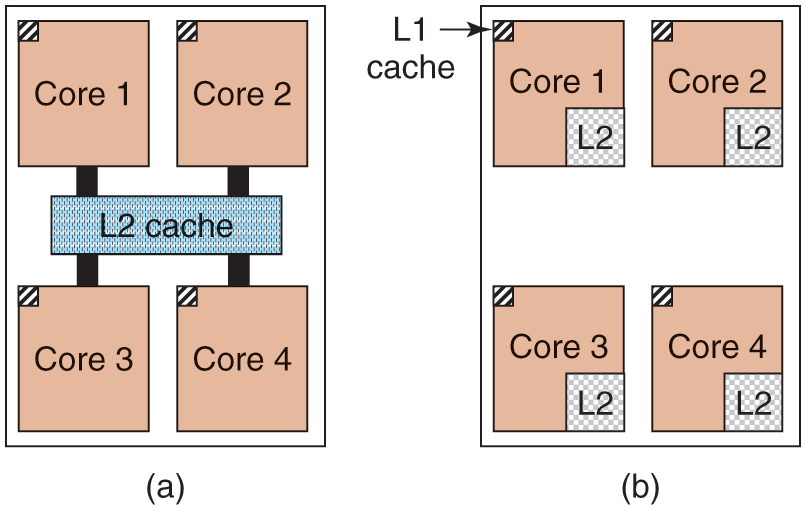
(a) A quad-core chip with a shared L2 cache. (b) A quad-core chip with separate L2 caches.
Incidentally, in terms of sheer numbers, nothing beats a modern GPU (Graphics Processing Unit). A GPU is a processor with, literally, thousands of tiny cores. They are very good for many small computations done in parallel, like rendering polygons in graphics applications. They are not so good at serial tasks. They are also hard to program. While GPUs can be useful for operating systems (e.g., for encryption or processing of network traffic), it is not likely that much of the operating system itself will run on the GPUs.
1.3.2 Memory
The second major component in any computer is the memory. Ideally, memory should be extremely fast (faster than executing an instruction so that the CPU is not held up by the memory), abundantly large, and dirt cheap. No current technology satisfies all of these goals, so a different approach is taken. The memory system is constructed as a hierarchy of layers, as shown in Fig. 1-9, which would be typical for a desktop computer or a server (notebooks use SSDs). The top layers have higher speed, smaller capacity, and greater cost per bit than the lower ones, often by factors of a billion or more.
Figure 1-9
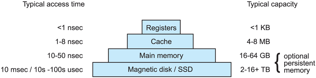
A typical memory hierarchy. The numbers are very rough approximations.
The top layer consists of the registers internal to the CPU. They are made of the same material as the CPU and are thus just as fast as the CPU. Consequently, there is no delay in accessing them. The storage capacity available in them is on the order of bits on a 32-bit CPU and bits on a 64-bit CPU. Less than 1 KB in both cases. Programs must manage the registers (i.e., decide what to keep in them) themselves, in software.
Next comes the cache memory, which is mostly controlled by the hardware. Main memory is divided up into cache lines, typically 64 bytes, with addresses 0 to 63 in cache line 0, 64 to 127 in cache line 1, and so on. The most heavily used cache lines are kept in a high-speed cache located inside or very close to the CPU. When the program needs to read a memory word, the cache hardware checks to see if the line needed is in the cache. If it is, called a cache hit, the request is satisfied from the cache and no memory request is sent over the bus to the main memory. Cache hits normally take only a few clock cycles. Cache misses have to go to memory, with a substantial time penalty of tens to hundreds of cycles. Cache memory is limited in size due to its high cost. Some machines have two or even three levels of cache, each one slower and bigger than the one before it.
Caching plays a major role in many areas of computer science, not just caching lines of RAM. Whenever a resource can be divided into pieces, some of which are used much more heavily than others, caching is often used to improve performance. Operating systems use it all the time. For example, most operating systems keep (pieces of) heavily used files in main memory to avoid having to fetch them from stable storage repeatedly. Similarly, the results of converting long path names like
/home/ast/projects/minix3/src/kernel/clock.c
into a ‘‘disk address’’ for the SSD or disk where the file is located can be cached to avoid repeated lookups. Finally, when the address of a Web page (URL) is converted to a network address (IP address), the result can be cached for future use. Many other uses exist.
In any caching system, several questions come up fairly soon, including:
When to put a new item into the cache.
Which cache line to put the new item in.
Which item to remove from the cache when a slot is needed.
Where to put a newly evicted item in the larger memory.
Not every question is relevant to every caching situation. For caching lines of main memory in the CPU cache, a new item will generally be entered on every cache miss. The cache line to use is generally computed by using some of the high-order bits of the memory address referenced. For example, with 4096 cache lines of 64 bytes and 32 bit addresses, bits 6 through 17 might be used to specify the cache line, with bits 0 to 5 the byte within the cache line. In this case, the item to remove is the same one as the new data goes into, but in other systems it might not be. Finally, when a cache line is rewritten to main memory (if it has been modified since it was cached), the place in memory to rewrite it to is uniquely determined by the address in question.
Caches are such a good idea that modern CPUs have two or more of them. The first level or L1 cache is always inside the CPU and usually feeds decoded instructions into the CPU’s execution engine. Most chips have a second L1 cache for very heavily used data words. The L1 caches are typically 32 KB each. In addition, there is often a second cache, called the L2 cache, that holds several megabytes of recently used memory words. The difference between the L1 and L2 caches lies in the timing. Access to the L1 cache is done without any delay, whereas access to the L2 cache involves a delay of several clock cycles.
On multicore chips, the designers have to decide where to place the caches. In Fig. 1-8(a), a single L2 cache is shared by all the cores. In contrast, in Fig. 1-8(b), each core has its own L2 cache. Each strategy has its pros and cons. For example, the shared L2 cache requires a more complicated cache controller but the per-core L2 caches makes keeping the caches consistent more difficult.
Main memory comes next in the hierarchy of Fig. 1-9. This is the workhorse of the memory system. Main memory is usually called RAM (Random Access Memory). Old-timers sometimes call it core memory, because computers in the 1950s and 1960s used tiny magnetizable ferrite cores for main memory. They have been gone for decades but the name persists. Currently, memories are often tens of gigabytes on desktop or server machines. All CPU requests that cannot be satisfied out of the cache go to main memory.
In addition to the main memory, many computers have different kinds of nonvolatile random-access memory. Unlike RAM, nonvolatile memory does not lose its contents when the power is switched off. ROM (Read Only Memory) is programmed at the factory and cannot be changed afterward. It is fast and inexpensive. On some computers, the bootstrap loader used to start the computer is contained in ROM. EEPROM (Electrically Erasable PROM) is also nonvolatile, but in contrast to ROM can be erased and rewritten. However, writing it takes orders of magnitude more time than writing RAM, so it is used in the same way ROM is, except that it is now possible to correct bugs in programs by rewriting them in the field. Boot strapping code may also be stored in Flash memory, which is similarly nonvolatile, but in contrast to ROM can be erased and rewritten. The boot strapping code is commonly referred to as BIOS (Basic Input/Output System). Flash memory is also commonly used as the storage medium in portable electronic devices such as smartphones and in SSDs to serve as a faster alternative to hard disks. Flash memory is intermediate in speed between RAM and disk. Also, unlike disk memory, if it is erased too many times, it wears out. Firmware inside the device tries to mitigate this through load balancing.
Yet another kind of memory is CMOS, which is volatile. Many computers use CMOS memory to hold the current time and date. The CMOS memory and the clock circuit that increments the time in it are powered by a small battery, so the time is correctly updated, even when the computer is unplugged. The CMOS memory can also hold the configuration parameters, such as which drive to boot from. CMOS is used because it draws so little power that the original factory-installed battery often lasts for several years. However, when it begins to fail, the computer can appear to be losing its marbles, forgetting things that it has known for years, like how to boot.
Incidentally, many computers today support a scheme known as virtual memory, which we will discuss at some length in Chap. 3. It makes it possible to run programs larger than physical memory by placing them on nonvolatile storage (SSD or disk) and using main memory as a kind of cache for the most heavily executed parts. From time to time, the program will need data that are currently not in memory. It frees up some memory (e.g., by writing some data that have not been used recently back to SSD or disk) and then loads the new data at this location. Because the physical address for the data and code is now no longer fixed, the scheme remaps memory addresses on the fly to convert the address the program generated to the physical address in RAM where the data are currently located. This mapping is done by a part of the CPU called the MMU (Memory Management Unit), as shown in Fig. 1-6.
The MMU can have a major impact on performance as every memory access by the program must be remapped using special data structures that are also in memory. In a multiprogramming system, when switching from one program to another, sometimes called a context switch, these data structures must change as the mappings differ from process to process. Both the on-the-fly address translation and the context switch can be expensive operations.
1.3.3 Nonvolatile Storage
Next in the hierarchy are magnetic disks (hard disks), solid state drives (SSDs), and persistent memory. Starting with the oldest and slowest, hard disk storage is two orders of magnitude cheaper than RAM per bit and often two orders of magnitude larger as well. The only problem is that the time to randomly access data on it is close to three orders of magnitude slower. The reason is that a disk is a mechanical device, as shown in Fig. 1-10.
Figure 1-10
Structure of a disk drive.
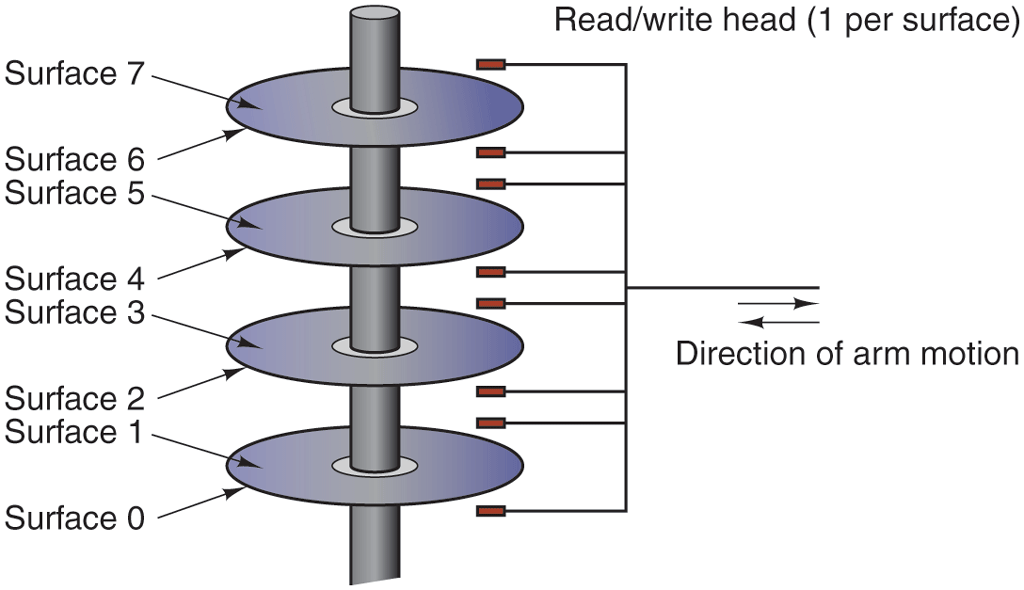
A disk consists of one or more metal platters that rotate at 5400, 7200, 10,800, 15,000 RPM or more. A mechanical arm pivots over the platters from the corner, similar to the pickup arm on an old 33-RPM phonograph for playing vinyl records. Information is written onto the disk in a series of concentric circles. At any given arm position, each of the heads can read an annular region known as a track. Together, all the tracks for a given arm position form a cylinder.
Each track is divided into some number of sectors, typically 512 bytes per sector. On modern disks, the outer cylinders contain more sectors than the inner ones. Moving the arm from one cylinder to the next takes about 1 msec. Moving it to a random cylinder typically takes 5–10 msec, depending on the drive. Once the arm is on the correct track, the drive must wait for the needed sector to rotate under the head, an additional delay of 5–10 msec, depending on the drive’s RPM. Once the sector is under the head, reading or writing occurs at a rate of 50 MB/sec on lowend disks to 160–200 MB/sec on faster ones.
Many people also refer to SSDs as disks, even though they are physically not disks at all and do not have platters or moving arms. They store data in electronic (Flash) memory. The only way in which they resemble disks in terms of hardware is that they also store a lot of data which is not lost when the power is off. But from the operating system’s point of view, they are somewhat disk-like. SSDs are much more expensive than rotating disks in terms of cost per byte stored, which is why they are not so much used in data centers for bulk storage. However, they are much faster than magnetic disks and since they have no mechanical arm to move, they are better at accessing data at random locations. Reading data from an SSD takes tens of microseconds instead of milliseconds as with hard disks. Writes are more complicated as they require a full data block to be erased first and take more time. But even if a write takes a few hundred microseconds, this is still better than a hard disk’s performance.
The youngest and fastest member of the stable storage family is known as persistent memory. The best known example is Intel Optane which became available in 2016. In many ways, persistent memory can be seen as an additional layer between SSDs (or hard disks) and memory: it is both fast, only slightly slower than regular RAM, and it holds its content across power cycles. While it can be used to implement really fast SSDs, manufacturers may also attach it directly to the memory bus. In fact, it can be used like normal memory to store an application’s data structures, except that the data will still be there when the power goes off. In that case, accessing it requires no special driver and may happen at byte granularity, obviating the need to transfer data in large blocks as in hard disks and SSDs.
1.3.4 I/O Devices
It should now be clear that CPU and memory are not the only resources that the operating system must manage. There are many other ones. Besides disks there many other I/O devices that interact heavily with the operating system. As we saw in Fig. 1-6, I/O devices generally consist of two parts: a controller and the device itself. The controller is a chip (or a set of chips) that physically controls the device. It accepts commands from the operating system, for example, to read data from the device, and carries them out.
In many cases, the actual control of the device is complicated and detailed, so it is the job of the controller to present a simpler (but still very complex) interface to the operating system. For example, a hard disk controller might accept a command to read sector 11,206 from disk 2. The controller then has to convert this linear sector number to a cylinder, sector, and head. This conversion may be complicated by the fact that outer cylinders have more sectors than inner ones and that some bad sectors have been remapped onto other ones. Then the controller has to determine which cylinder the disk arm is on and give it a command to move in or out the requisite number of cylinders. It has to wait until the proper sector has rotated under the head and then start reading and storing the bits as they come off the drive, removing the preamble and computing the checksum. Finally, it has to assemble the incoming bits into words and store them in memory. To do all this work, controllers often contain small embedded computers that are programmed to do their work.
The other piece is the actual device itself. Devices have fairly simple interfaces, both because they cannot do much and to make them standard. The latter is needed so that any SATA disk controller can handle any SATA disk, for example. SATA stands for Serial ATA and ATA in turn stands for AT Attachment. In case you are curious what AT stands for, this was IBM’s second generation ‘‘Personal Computer Advanced Technology’’ built around the then-extremely-potent 6-MHz 80286 processor that the company introduced in 1984. What we learn from this is that the computer industry has a habit of continuously enhancing existing acronyms with new prefixes and suffixes. We also learned that an adjective like ‘‘advanced’’ should be used with great care, or you will look silly 40 years down the line.
SATA is currently the standard type of hard disk on many computers. Since the actual device interface is hidden behind the controller, all that the operating system sees is the interface to the controller, which may be quite different from the interface to the device.
Because each type of controller is different, different software is needed to control each one. The software that talks to a controller, giving it commands and accepting responses, is called a device driver. Each controller manufacturer has to supply a driver for each operating system it supports. Thus a scanner may come with drivers for macOS, Windows 11, and Linux, for example.
To be used, the driver has to be put into the operating system so it can run in kernel mode. Drivers can actually run outside the kernel, and operating systems like Linux and Windows nowadays do offer some support for doing so, but the vast majority of the drivers still run below the kernel boundary. Only very few current systems, such as MINIX 3 run all drivers in user space. Drivers in user space must be allowed to access the device in a controlled way, which is not straightforward without some hardware support.
There are three ways the driver can be put into the kernel. The first way is to relink the kernel with the new driver and then reboot the system. Many older UNIX systems work like this. The second way is to make an entry in an operating system file telling it that it needs the driver and then reboot the system. At boot time, the operating system goes and finds the drivers it needs and loads them. Older versions of Windows work this way. The third way is for the operating system to be able to accept new drivers while running and install them on the fly without the need to reboot. This way used to be rare but is becoming much more common now. Hot-pluggable devices, such as USB and Thunderbolt devices (discussed below), always need dynamically loaded drivers.
Every controller has a small number of registers that are used to communicate with it. For example, a minimal disk controller might have registers for specifying the disk address, memory address, sector count, and direction (read or write). To activate the controller, the driver gets a command from the operating system, then translates it into the appropriate values to write into the device registers. The collection of all the device registers forms the I/O port space, a subject we will come back to in Chap. 5.
On some computers, the device registers are mapped into the operating system’s address space (the addresses it can use), so they can be read and written like ordinary memory words. On such computers, no special I/O instructions are required and user programs can be kept away from the hardware by not putting these memory addresses within their reach (e.g., by using base and limit registers). On other computers, the device registers are put in a special I/O port space, with each register having a port address. On these machines, special IN and OUT instructions are available in kernel mode to allow drivers to read and write the registers. The former scheme eliminates the need for special I/O instructions but uses up some of the address space. The latter uses no address space but requires special instructions. Both systems are widely used.
Input and output can be done in three different ways. In the simplest method, a user program issues a system call, which the kernel then translates into a procedure call to the appropriate driver. The driver then starts the I/O and sits in a tight loop continuously polling the device to see if it is done (usually there is some bit that indicates that the device is still busy). When the I/O has completed, the driver puts the data (if any) where they are needed and returns. The operating system then returns control to the caller. This method is called busy waiting and has the disadvantage of tying up the CPU polling the device until it is finished.
The second method is for the driver to start the device and ask it to give an interrupt when it is finished. At that point, the driver returns. The operating system then blocks the caller if need be and looks for other work to do. When the controller detects the end of the transfer, it generates an interrupt to signal completion.
Interrupts are very important in operating systems, so let us examine the idea more closely. In Fig. 1-11(a) we see a three-step process for I/O. In step 1, the driver tells the controller what to do by writing into its device registers. The controller then starts the device. When the controller has finished reading or writing the number of bytes it has been instructed to transfer, it signals the interrupt controller chip using certain bus lines in step 2. If the interrupt controller is ready to accept the interrupt (which it may not be if it is busy handling a higher-priority interrupt), it asserts a pin on the CPU chip telling it, in step 3. In step 4, the interrupt controller puts the number of the device on the bus so the CPU can read it and know which device has just finished (many devices may be running at the same time).
Figure 1-11
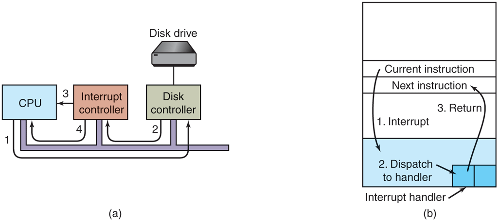
(a) The steps in starting an I/O device and getting an interrupt. (b) Interrupt processing involves taking the interrupt, running the interrupt handler, and returning to the user program.
Once the CPU has decided to take the interrupt, the program counter and PSW are typically then pushed onto the current stack and the CPU switched into kernel mode. The device number may be used as an index into part of memory to find the address of the interrupt handler for this device. This part of memory is called the interrupt vector table. Once the interrupt handler (part of the driver for the interrupting device) has started, it saves the stacked program counter, PSW, and other registers (typically in the process table). Then it queries the device to learn its status. When the handler is all finished, it restores the context and returns to the previously running user program to the first instruction that was not yet executed. These steps are shown in Fig. 1-11(b). We will discuss interrupt vectors further in in the next chapter.
The third method for doing I/O makes use of special hardware: a DMA (Direct Memory Access) chip that can control the flow of bits between memory and some controller without constant CPU intervention. The CPU sets up the DMA chip, telling it how many bytes to transfer, the device and memory addresses involved, and the direction, and lets it go. When the DMA chip is done, it causes an interrupt, which is handled as described above. DMA and I/O hardware in general will be discussed in more detail in Chap. 5.
1.3.5 Buses
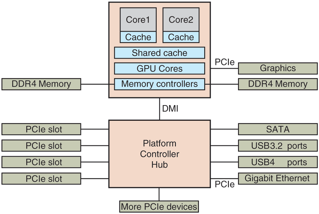
The organization of Fig. 1-6 was used on minicomputers for years and also on the original IBM PC. However, as processors and memories got faster, the ability of a single bus (and certainly the IBM PC bus) to handle all the traffic was strained to the breaking point. Something had to give. As a result, additional buses were added, both for faster I/O devices and for CPU-to-memory traffic. As a consequence of this evolution, a large x86 system currently looks something like Fig. 1-12.
Figure 1-12
The structure of a large x86 system.
This system has many buses (e.g., cache, memory, PCIe, PCI, USB, SATA, and DMI), each with a different transfer rate and function. The operating system must be aware of all of them for configuration and management. The main bus is the PCIe (Peripheral Component Interconnect Express) bus.
The PCIe bus was invented by Intel as a successor to the older PCI bus, which in turn was a replacement for the original ISA (Industry Standard Architecture) bus. Capable of transferring tens of gigabits per second, PCIe is much faster than its predecessors. It is also very different in nature. Up to its creation in 2004, most buses were parallel and shared. A shared bus architecture means that multiple devices use the same wires to transfer data. Thus, when multiple devices have data to send, you need an arbiter to determine who can use the bus. In contrast, PCIe makes use of dedicated, point-to-point connections. A parallel bus architecture as used in traditional PCI means that you send each word of data over multiple wires. For instance, in regular PCI buses, a single 32-bit number is sent over 32 parallel wires. In contrast to this, PCIe uses a serial bus architecture and sends all bits in a message through a single connection, known as a lane, much like a network packet. This is much simpler because you do not have to ensure that all 32 bits arrive at the destination at exactly the same time. Parallelism is still used, because you can have multiple lanes in parallel. For instance, we may use 32 lanes to carry 32 messages in parallel. As the speed of peripheral devices like network cards and graphics adapters increases rapidly, the PCIe standard is upgraded every 3–5 years. For instance, 16 lanes of PCIe 4.0 offer 256 gigabits per second. Upgrading to PCIe 5.0 will give you twice that speed and PCIe 6.0 will double that again. Meanwhile, we still have legacy devices for the older PCI standard. These devices can be hooked up to a separate hub processor.
In this configuration, the CPU talks to memory over a fast DDR4 bus, to an external graphics device over PCIe and to all other devices via a hub over a DMI (Direct Media Interface) bus. The hub in turn connects all the other devices, using the Universal Serial Bus to talk to USB devices, the SATA bus to interact with hard disks and DVD drives, and PCIe to transfer Ethernet frames. We have already mentioned the older PCI devices that use a traditional PCI bus.
Moreover, each of the cores has a dedicated cache and a much larger cache that is shared between them. Each of these caches introduces yet another bus.
The USB (Universal Serial Bus) was invented to attach all the slow I/O devices, such as the keyboard and mouse, to the computer. However, calling a modern USB4 device humming along at 40 Gbps ‘‘slow’’ may not come naturally for the generation that grew up with 8-Mbps ISA as the main bus in the first IBM PCs. USB uses a small connector with 4–11 wires (depending on the version), some of which supply electrical power to the USB devices or connect to ground. USB is a centralized bus in which a root device polls all the I/O devices every 1 msec to see if they have any traffic. USB 1.0 could handle an aggregate load of 12 Mbps, USB 2.0 increased the speed to 480 Mbps, USB 3.0 to 5 Gbps, USB 3.2 to 20 Gbps and USB 4 will double that. Any USB device can be connected to a computer and it will function immediately, without requiring a reboot, something pre-USB devices required, much to the consternation of a generation of frustrated users.
1.3.6 Booting the Computer
Very briefly, the boot process is as follows. Every PC contains a motherboard, which contains the CPU, slots for memory chips, and sockets for PCIe (or other) plug-in cards. On the motherboard a small amount of flash holds a program called the system firmware, which we commonly still refer to as the BIOS (Basic Input Output System), even though strictly speaking the name BIOS applies only to the firmware in somewhat older IBM PC compatible machines. Booting using the original BIOS was slow, architecture-dependent, and limited to smaller SSDs and disks (up to 2 TB). It was also very easy to understand. When Intel proposed what would become UEFI (Unified Extensible Firmware Interface) as a replacement, it remedied all these issues: UEFI allows for fast booting, different architectures, and storage sizes up to 8 ZiB, or bytes. It is also so complex that trying to understand it fully has sucked the happiness out of many a life. In this chapter, we will cover both old and new style BIOS firmware, but only the essentials.
After we press the power button, the motherboard waits for the signal that the power supply has stabilized. When the CPU starts executing, it fetches code from a hard-coded physical address (known as the reset vector) that is mapped to the flash memory. In other words, it executes code from the BIOS which detects and initializes various resources, such as RAM, the Platform Controller Hub (see Fig. Fig. 1-12), and interrupt controllers. In addition, it scans the PCI and/or PCIe buses to detect and initialize all devices attached to them. If the devices present are different from when the system was last booted, it also configures the new devices. Finally, it sets up the runtime firmware which offers critical services (including low-level I/O) that can be used by the system after booting.
Next, it is time to move to the next stage of the booting process. In systems using the old-style BIOS, this was all very straightforward. The BIOS would determine the boot device by trying a list of devices stored in the CMOS memory. The user can change this list by entering a BIOS configuration program just after booting. For instance, you may ask the system to attempt to boot from a USB drive, if one is present. If that fails, the system boots from the hard disk or SSD. The first sector from the boot device is read into memory and executed. This sector, known as the MBR (Master Boot Record), contains a program that normally examines the partition table at the end of the boot sector to determine which partition is active. A partition is a distinct region on the storage device that may for instance contain its own file systems. Then a secondary boot loader is read in from that partition. This loader reads in the operating system from the active partition and starts it. The operating system then queries the BIOS to get the configuration information. For each device, it checks to see if it has the device driver. If not, it asks the user to install it, for instance by downloading it from the Internet. Once it has all the device drivers, the operating system loads them into the kernel. Then it initializes its tables, creates whatever background processes are needed, and starts up a login program or GUI.
With UEFI, things are different. First, it no longer relies on a Master Boot Record residing in the first sector of the boot device, but it looks for the location of the partition table in the second sector of the device. This GPT (GUID Partition Table) contains information about the location of the various partitions on the SSD or disk. Second, the BIOS itself has enough functionality to read file systems of specific types. According to the UEFI standard, it should support at least the FAT-12, FAT-16, and FAT-32 types. One such file system is placed in a special partition, known as the EFI system partition (ESP). Rather than a single magic boot sector, the boot process can now use a proper file system containing programs, configuration files, and anything else that may be useful during boot. Moreover, UEFI expects the firmware to be able to execute programs in a specific format, called PE (Portable Executable). As you can see, the BIOS under UEFI very much looks like a little operating system itself which understands partitions, file systems, executables, etc. It even has a shell with some standard commands.
The boot code still needs to pick one of the bootloader programs to load Linux or Windows, or whatever operating system, but there may be many partitions with operating systems and given so much choice, which one should it pick? This is decided by the UEFI boot manager, which you can think of as a boot menu with different entries and a configurable order in which to try the different boot options. Changing the menu and the default bootloader is very easy and can be done from within the currently executing operating system. As before, the bootloader will continue loading the operating system of choice.
This is by no means the full story. UEFI is very flexible and highly standardized, and contains many advanced features. However, this is enough for now. In Chap. 9, we will pick up UEFI again when we discuss an interesting feature known as Secure Boot, which allows a user to be sure that the operating system is booted as intended and with the correct software.